Open-source semiconductor process simulation
Virtual fabrication, device modeling, and packaging analysis in one browser-native platform.
FabForge combines 3D process simulation, device TCAD, advanced packaging workflows, sign-off analytics, and API-first deployment into a single system built for fabless teams, foundries, OSATs, and research groups.
Featured simulation
3nm FinFET process evolution
Full process, packaging, API, and simulation stack.
Examples spanning interconnect, advanced nodes, packaging, and MEMS.
Platform surface
What FabForge puts in one workflow
FabForge is designed as a platform rather than a point tool, so process simulation, packaging analysis, and deployment automation share the same data model and runtime.
3D process simulation
Deposition, etch, CMP, lithography, oxidation, diffusion, and implant flows in a recipe-driven environment.
Device TCAD
Electrical I-V and C-V workflows connect process results to device behavior through DEVSIM-backed solving.
Advanced packaging
Model warpage, fatigue, underfill, and interconnect structures across HDI, flip-chip, and chiplet-oriented stacks.
GPU-accelerated analysis
Scale demanding workflows with CuPy, cuDSS, AmgX, and multi-tier FEA strategies instead of CPU-only bottlenecks.
API-first deployment
Expose simulation services through REST, gRPC, and WebSocket interfaces for cloud, on-prem, and hybrid flows.
Browser-native collaboration
Bring simulation into a modern web UI instead of isolated workstation installs and opaque desktop-only environments.
Customer value
Why engineering and commercial teams care
FabForge compresses fragmented simulation workflows into a single system that is easier to deploy, easier to extend, and easier to expose to the rest of the engineering organization.
Lower access barrier
Give advanced process modeling to teams that cannot justify six-figure annual commercial seat costs.
Faster iteration loops
Evaluate geometry, process recipes, packaging structures, and device response without bouncing between disconnected tools.
Deployment flexibility
Run FabForge in the browser, in Docker, behind internal APIs, or in a multi-tenant SaaS environment.
Open extensibility
Keep source visibility, integrate custom physics, and build internal workflows without black-box vendor lock-in.
Visual proof
Real FabForge simulation outputs
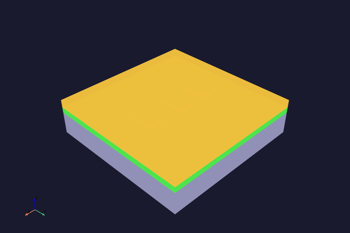
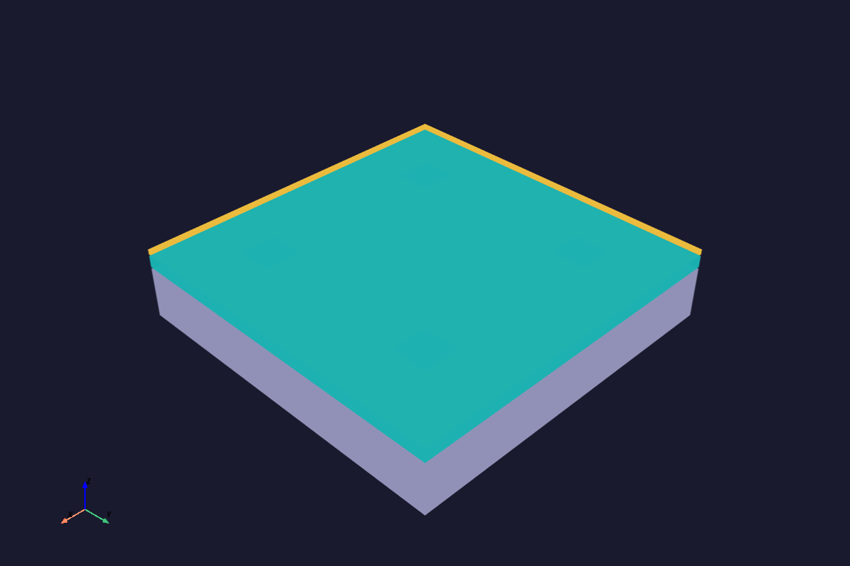
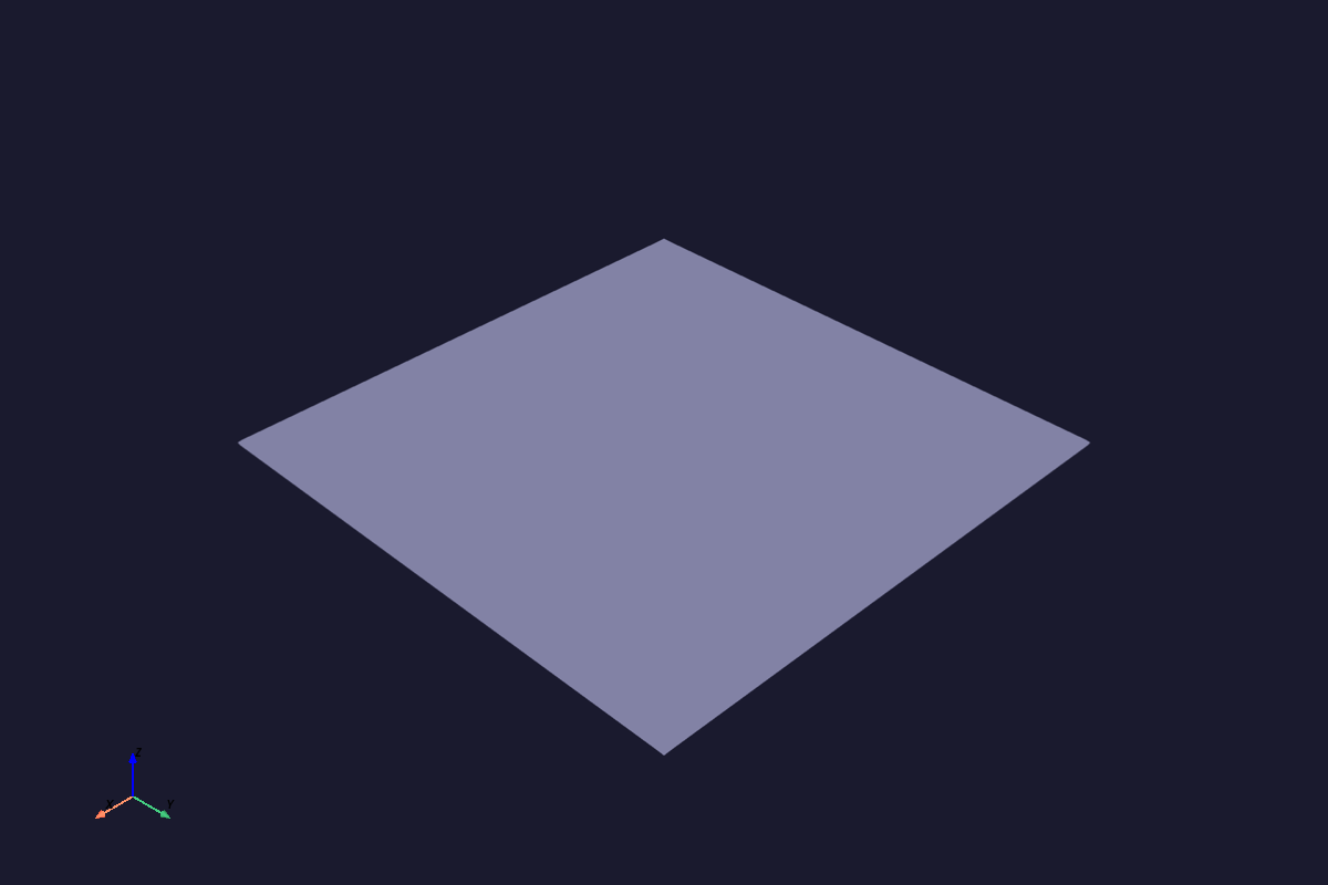
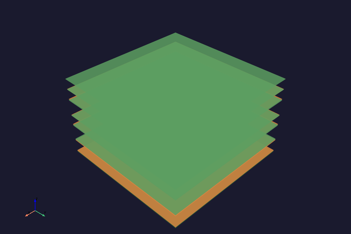
These media blocks are drawn from actual FabForge process runs, showing how recipes progress from substrate to complex structures.
3nm process clip
TSMC N3-class GAA nanosheet
Shows stacked nanosheet formation, inner-spacer evolution, channel release, and wrap-around gate fill.
18A process clip
Intel 18A RibbonFET + PowerVia
Highlights nanoribbon evolution, advanced gate fill, and backside power delivery modules in a short process clip.
Packaging clip
Fine-pitch flip-chip packaging
Highlights FabForge coverage beyond wafer processing into advanced packaging structures.
Economic impact
A different cost model for advanced process simulation
Commercial process simulation software often lands in the $50,000 to $200,000 per-seat annual range. FabForge changes the economics with an open-source core, browser delivery, and cloud or on-prem deployment options.
Typical commercial seat range
Benchmark cost level for established process simulation platforms in the market.
Corporate-equivalent rebuild cost
Estimated cost for a conventional team to reproduce a comparable multi-surface platform.
Typical enterprise delivery window
Reference timeline FabForge compresses through an integrated architecture and AI-assisted development.
Legacy model
- Per-seat licensing and workstation installs
- Limited APIs and slower internal integration
- Separate tools for process, packaging, and downstream analytics
FabForge model
- Browser-native access with open-source core
- REST, gRPC, and WebSocket service interfaces
- Unified simulation stack for wafer, device, and packaging workflows
Who it serves
Built for engineering organizations that need control
Fabless teams
Bring process-aware design review closer to the product team without requiring full fab-resident tool stacks.
Foundries and IDMs
Deploy an internal platform you can extend, secure, and integrate with proprietary data pipelines.
Packaging groups
Simulate HDI, flip-chip, and reliability-oriented structures in the same platform as process flows.
Research labs
Open advanced semiconductor simulation to teams priced out of traditional licensing models.
Team
Built by operators, engineers, and domain specialists
FabForge brings together semiconductor equipment leadership, applied mathematics, software development, and industry operating experience.
Product Chief
Kevin
Account Manager for Intel, GM and USA Country Manager for a leading semi equipment component company, achieved revenue increasing 5x in 4 yrs; Engineer at Lam Research. Patent Inventor; MSME at Univ of Cincinnati; ML and Data Science Certificates, Harvard Univ Online.
Developer
Alex
Applied Math & CS degree, UC Berkeley.
Team Member
To Be Announced
Additional FabForge team information will be announced as the organization expands.
Advisor
David
Former VP of Etch Product and GM of Asia Pacific at Applied Materials Inc, former CEO of SMIC, Founding Chairman of YMTC.